| CPC H01L 29/0665 (2013.01) [H01L 29/0847 (2013.01); H01L 29/4236 (2013.01)] | 19 Claims |

|
1. A semiconductor device comprising:
a substrate;
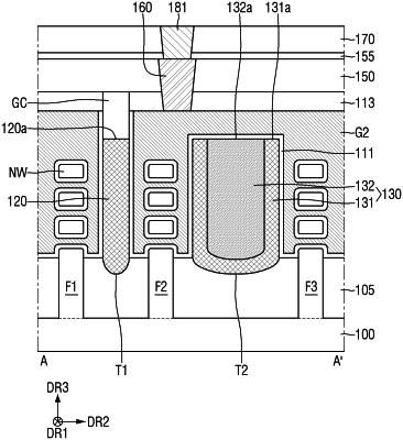
a first active pattern which extends in a first horizontal direction on the substrate, and comprises a first side wall and a second side wall opposite to the first side wall in a second horizontal direction different from the first horizontal direction;
a second active pattern which extends in the first horizontal direction on the first side wall of the first active pattern;
a third active pattern which extends in the first horizontal direction on the second side wall of the first active pattern;
a first insulating structure in a first trench extending in the first horizontal direction on the first side wall of the first active pattern;
a second insulating structure in a second trench extending in the first horizontal direction on the second side wall of the first active pattern, and comprising a first insulating layer on side walls and on a bottom surface of the second trench, and a second insulating layer in the second trench on the first insulating layer;
a gate-cut extending in the first horizontal direction on the first insulating structure; and
a gate electrode extending in the second horizontal direction on the first active pattern,
wherein the first insulating layer and the second insulating layer comprise different materials from each other,
wherein the first insulating structure and the first insulating layer comprise a same material,
wherein an upper surface of the first insulating structure is on a same plane as an upper surface of the second insulating layer, and
wherein a distance in the second horizontal direction between the second active pattern and the first active pattern is less than a distance in the second horizontal direction between the first active pattern and the third active pattern.
|