US 11,869,936 B2
Semiconductor device and method of forming the semiconductor device
Marc Adam Bergendahl, Troy, NY (US); Gauri Karve, Cohoes, NY (US); Fee Li Lie, Albany, NY (US); Eric R. Miller, Watervliet, NY (US); Robert Russell Robison, Rexford, NY (US); John Ryan Sporre, Albany, NY (US); and Sean Teehan, Rensselaer, NY (US)
Assigned to International Business Machines Corporation, Armonk, NY (US)
Filed by International Business Machines Corporation, Armonk, NY (US)
Filed on Aug. 14, 2021, as Appl. No. 17/402,507.
Application 16/398,987 is a division of application No. 15/859,362, filed on Dec. 30, 2017, granted, now 10,381,437, issued on Aug. 13, 2019.
Application 15/859,362 is a division of application No. 15/294,490, filed on Oct. 14, 2016, granted, now 9,917,196, issued on Mar. 13, 2018.
Application 17/402,507 is a continuation of application No. 16/398,987, filed on Apr. 30, 2019, granted, now 11,127,815.
Prior Publication US 2021/0376078 A1, Dec. 2, 2021
This patent is subject to a terminal disclaimer.
Int. Cl. H01L 21/00 (2006.01); H01L 29/06 (2006.01); H01L 29/423 (2006.01); H01L 29/66 (2006.01); H01L 29/786 (2006.01)
CPC H01L 29/0657 (2013.01) [H01L 29/42392 (2013.01); H01L 29/66742 (2013.01); H01L 29/78642 (2013.01); H01L 29/78648 (2013.01); H01L 29/78696 (2013.01)] 16 Claims
OG exemplary drawing
 
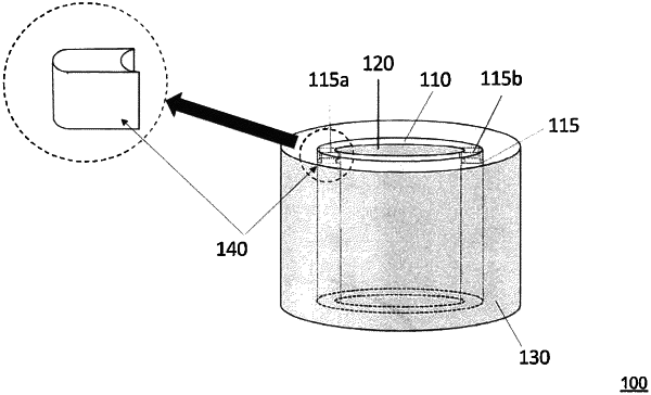
1. A semiconductor device comprising:
a fin structure including a recess formed in an upper surface of the fin structure;
a conductor formed in an upper surface of the fin structure;
an inner gate formed in the recess of the fin structure; and
an outer gate formed outside and around the fin structure.