| CPC H01L 29/0646 (2013.01) [H01L 21/265 (2013.01); H01L 21/761 (2013.01); H01L 23/5223 (2013.01); H01L 23/5227 (2013.01); H01L 23/5286 (2013.01); H01L 24/05 (2013.01); H01L 27/0676 (2013.01); H01L 28/10 (2013.01); H01L 28/20 (2013.01); H01L 28/40 (2013.01); H01L 28/60 (2013.01); H01L 2224/48463 (2013.01)] | 20 Claims |
|
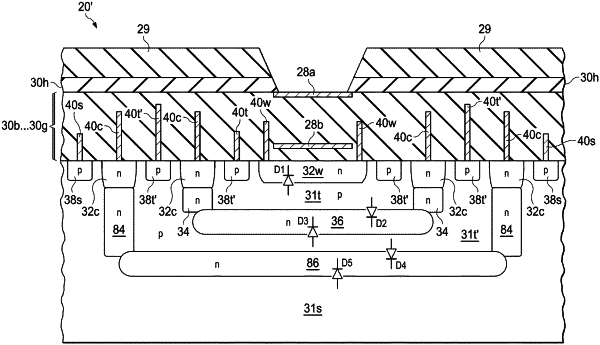
1. A method of forming an integrated circuit, comprising:
forming a first terminal over a semiconductor substrate having a first conductivity type;
forming a second terminal between the first terminal and a surface of the semiconductor substrate, the first terminal being separated from the second terminal by a dielectric layer;
forming a first p-n junction between the semiconductor substrate and the second terminal, the first p-n junction having a first orientation with respect to the substrate surface;
forming a second p-n junction between the first p-n junction and the second terminal, the second p-n junction having a second opposite orientation with respect to the substrate surface; and
forming a third p-n junction between the second p-n junction and the second terminal, the third p-n junction have the first orientation.
|