| CPC H01L 27/14627 (2013.01) [H01L 22/20 (2013.01); H01L 27/14685 (2013.01); H04N 25/40 (2023.01); H04N 25/702 (2023.01); H01L 27/1463 (2013.01); H01L 27/14621 (2013.01); H01L 27/14645 (2013.01)] | 20 Claims |
|
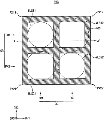
1. A pixel array of an image sensor, comprising:
a plurality of pixel groups, each pixel group comprising:
a plurality of unit pixels adjacent to each other and respectively including photoelectric conversion elements disposed in a semiconductor substrate;
a color filter shared by the plurality of unit pixels, so that the plurality of unit pixels are the same color pixels; and
a plurality of microlenses disposed on the color filter and having sizes different from each other, the plurality of microlenses configured to respectively focus an incident light to the photoelectric conversion elements included in the plurality of unit pixels.
|