| CPC H01L 27/1461 (2013.01) [H01L 27/14643 (2013.01); H01L 27/14689 (2013.01)] | 20 Claims |
|
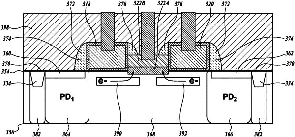
1. A pixel cell, comprising:
a semiconductor substrate having a front surface and a doped well region having a first conductivity type;
a first photodiode disposed in the semiconductor substrate adjacent to the doped well region, the first photodiode adapted to photogenerate image charge in response to incident light;
a second photodiode disposed in the semiconductor substrate adjacent to the doped well region, the second photodiode adapted to photogenerate image charge in response to incident light;
a first transfer gate disposed proximate to the front surface of the semiconductor substrate;
a second transfer gate disposed proximate to the front surface of the semiconductor substrate, the second transfer gate positioned a spaced distance from the first transfer gate;
a floating diffusion disposed in between the first transfer gate and the second transfer gate, the floating diffusion comprising a first floating diffusion layer disposed on the front surface of the semiconductor substrate adjacent to the doped well region and a second floating diffusion layer disposed on the first floating diffusion layer, the second floating diffusion layer having a second conductivity type opposite the first conductivity type of the doped well region, wherein both the first floating diffusion layer and the second floating diffusion layer are disposed laterally between the first transfer gate and the second transfer gate, and
wherein the first transfer gate and the second transfer gate are coupled to transfer the image charge from the first photodiode and the second photodiode to the second floating diffusion layer; and
a sidewall spacer disposed proximate to the first transfer gate or the second transfer gate, and wherein the second floating diffusion layer is disposed between the sidewall spacer and the first floating diffusion layer.
|