|
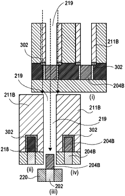
1. An integrated circuit structure, comprising: a fin comprising silicon; a gate stack over the fin, the gate stack comprising a gate dielectric and a gate electrode; a first dielectric spacer along and in contact with a first side of the gate stack, and a second dielectric spacer along and in contact with a second side of the gate stack, the first and second dielectric spacers over at least a portion of the fin; an insulating material vertically between and in contact with the portion of the fin and the first and second dielectric spacers, wherein the insulating material comprises a first dielectric material, and the first and second dielectric spacers comprise a second dielectric material different than the first dielectric material, and wherein the first dielectric material has a widest lateral width the same as a widest lateral width of the second dielectric material; a first epitaxial source or drain structure at the first side of the gate stack, and a second epitaxial source or drain structure at the second side of the gate stack; and a first tip laterally adjacent and in direct contact with the first epitaxial source or drain structure, and a second tip laterally adjacent and in direct contact with the second epitaxial source or drain structure, the first tip and the second tip vertically beneath and in direct contact with the first dielectric material of the insulating material and in simultaneous direct contact with the fin channel.
|