| CPC H01L 27/092 (2013.01) [H01L 21/76898 (2013.01); H01L 21/8221 (2013.01); H01L 21/823871 (2013.01); H01L 23/485 (2013.01); H01L 27/0688 (2013.01)] | 14 Claims |
|
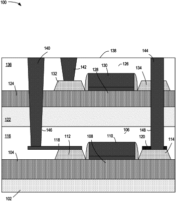
1. A method of forming an integrated circuit device structure comprising:
forming a first transistor;
forming a first dielectric layer over the first transistor;
forming a bonding layer over the first dielectric layer;
affixing a semiconductor layer to the bonding layer;
forming a second transistor comprising a channel portion of the semiconductor layer;
forming a second dielectric layer over the second transistor;
forming a first contact coupled with a source region or a drain region of the first transistor, wherein forming the first contact comprises forming an opening with a continuous sidewall that extends through the second dielectric layer, through the semiconductor layer, and through a thickness of the bonding layer that surrounds the first contact, to within the first dielectric layer, and lands upon a top surface of the source region or the drain region of the first transistor;
forming a second contact coupled with a source region or a drain region of the second transistor, wherein forming the second contact comprises forming a second opening with a continuous sidewall that extends through the second dielectric layer and lands upon a top surface of the source region or the drain region of the first transistor;
depositing metal concurrently into the first and second openings, the metal directly contacting the source region or the drain region of both the first and second transistors; and
planarizing a top surface of the metal within the first contact to be substantially coplanar with a top surface of the metal within the second contact.
|