| CPC H01L 27/0207 (2013.01) [G03F 1/36 (2013.01); G06F 30/398 (2020.01); H01L 23/552 (2013.01); H01L 27/11807 (2013.01); H01L 2027/11874 (2013.01); H01L 2027/11881 (2013.01); H01L 2027/11892 (2013.01)] | 20 Claims |
|
1. A method of designing a layout of a semiconductor device comprising:
receiving information indicating a size of a target chip;
allocating a first hard macro area, a second hard macro area and an input/output area;
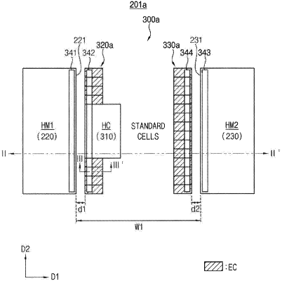
arranging a head cell, a plurality of first ending cells and a plurality of second ending cells in a standard cell area between the first hard macro area and the second hard macro area such that the head cell is not overlapped with the plurality of first ending cells and the plurality of second ending cells;
providing a substrate having an upper surface that extends in a first direction and a second direction that crosses the first direction;
providing a signal connection layer on the upper surface;
providing a power mesh layer on the signal connection layer; and
providing a via on the head cell and extending in a third direction through the signal connection layer to the power mesh layer, wherein the third direction is perpendicular to the upper surface and a power supply voltage applied to the first hard macro area by the head cell is provided from the power mesh layer through the via,
wherein the head cell is configured to perform power gating of the power supply voltage provided to at least one of the first hard macro area and the second hard macro area, and
wherein the second hard macro area is spaced apart from the first hard macro area in the first direction by a first distance.
|