| CPC H01L 24/43 (2013.01) [H01L 21/32139 (2013.01); H01L 21/76885 (2013.01); H01L 23/49827 (2013.01); H01L 23/49894 (2013.01); H01L 23/5226 (2013.01); H01L 23/5283 (2013.01); H01L 24/49 (2013.01); H01L 2221/1068 (2013.01)] | 7 Claims |
|
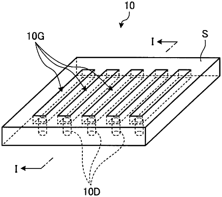
1. A wiring fabrication method, comprising:
pressing a first template, which includes a first recessed portion and a second recessed portion at a bottom of the first recessed portion, against a first film to form a first pattern including a first raised portion, corresponding to the first recessed portion, and a second raised portion, corresponding to the second recessed portion, the second raised portion protruding from the first raised portion;
forming a first wiring, corresponding to the first raised portion, and a via, corresponding to the second raised portion, the via protruding from the first wiring; and
forming a second wiring contacting the via, the via extending between the first wiring and the second wiring, wherein
forming the second wiring comprises:
forming a second conductive material film contacting the via;
forming a second film on the second conductive material film;
forming a second pattern in the second film; and
etching the second conductive material film using the second pattern as a mask to form the second wiring contacting the via.
|