| CPC H01L 24/08 (2013.01) [H01L 25/0657 (2013.01); H01L 25/18 (2013.01); G11C 5/025 (2013.01); H01L 2224/08145 (2013.01); H01L 2225/06506 (2013.01); H01L 2225/06562 (2013.01)] | 20 Claims |
|
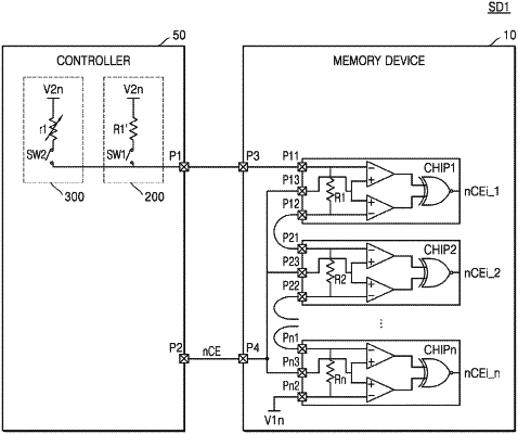
1. A storage device comprising:
a controller comprising first and second pins, and configured to output a multi-level chip enable signal through the second pin; and
a memory device comprising a third pin connected to the first pin and a fourth pin connected to the second pin, and a plurality of memory chips commonly connected to the fourth pin, the plurality of memory chips respectively comprising a plurality of resistors connected to each other in a daisy-chain structure between the third pin and a first voltage terminal,
wherein the plurality of memory chips are configured to respectively generate a plurality of reference voltage periods that divide between a voltage level of the third pin and a voltage level of the first voltage terminal based on the plurality of resistors, and
wherein when a voltage level of the multi-level chip enable signal corresponds to one of the plurality of reference voltage periods, a memory chip corresponding to the one reference voltage period is selected from among the plurality of memory chips.
|