| CPC H01L 23/562 (2013.01) [H01L 23/5226 (2013.01); H01L 23/5283 (2013.01); H01L 23/535 (2013.01); H01L 23/53257 (2013.01); H10B 43/27 (2023.02)] | 3 Claims |
|
1. A semiconductor storage device comprising:
a substrate;
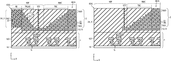
a first stacked body provided above the substrate, the first stacked body including a plurality of first insulating layers and a plurality of conductive layers alternately stacked in a first direction, the first stacked body including a first region and a second region next to the first region in a second direction crossing the first direction and having a staircase pattern;
a plurality of columnar portions passing through the first region of the first stacked body;
a second stacked body provided next to the second region of the first stacked body in the second direction and including the plurality of first insulating layers and the plurality of conductive layers alternately stacked in the first direction, the second stacked body having a staircase pattern;
a plurality of first slits extending through the first stacked body and the second stacked body in the second direction;
a third stacked body provided next to the second stacked body in the second direction, the third stacked body including the plurality of first insulating layers and a plurality of second insulating layers alternately stacked in the first direction, at least one of the plurality of the second insulating layers respectively connected to at least one of the plurality of conductive layers of the second stacked body;
an outer edge of the substrate provided next to the third stacked body in the second direction, wherein
the plurality of first insulating layers and the plurality of second insulating layers are different in material from each other,
wherein the third stacked body is a dummy stacked body that is not used for connection of word lines; and
a second slit, which extends in a direction intersecting the first slits, between the first stacked body and the second stacked body,
wherein the second stacked body is a dummy stacked body that is not used for connection of word lines;
a third insulating layer provided around the third stacked body,
wherein the first slits does not extend through the third stacked body,
wherein
the plurality of first insulating layers are silicon oxide film layers, and
the plurality of conductive layers are tungsten layers.
|