| CPC H01L 23/5226 (2013.01) [H01L 23/5383 (2013.01); H01L 23/5386 (2013.01); H01L 23/5389 (2013.01); H01L 23/53228 (2013.01); H01L 24/09 (2013.01); H01L 25/072 (2013.01); H01L 25/50 (2013.01); H01L 28/40 (2013.01); H01L 2224/0231 (2013.01); H01L 2224/02373 (2013.01); H01L 2224/02381 (2013.01)] | 20 Claims |
|
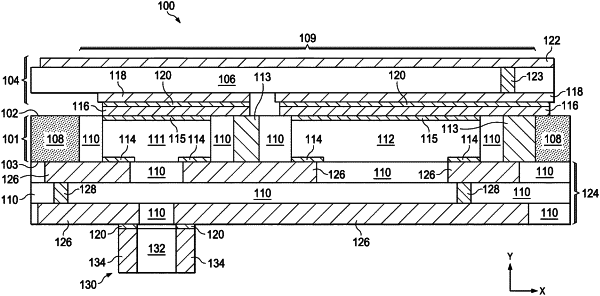
1. A method for fabricating a packaged electronic device, the method comprising:
attaching an organic panel frame to an adhesive carrier structure;
attaching a plurality of semiconductor dies to the adhesive carrier structure in openings of the organic panel frame;
forming a lamination structure in gaps between the organic panel frame and the semiconductor dies;
removing the adhesive carrier structure;
forming a redistribution layer (RDL) structure with a conductive structure electrically connected to contact structures of the semiconductor dies;
attaching a ceramic substrate to the semiconductor dies; and
separating a packaged electronic device from the panel.
|