| CPC H01L 23/5226 (2013.01) [H01L 23/5283 (2013.01); H10B 41/27 (2023.02); H10B 43/27 (2023.02)] | 8 Claims |
|
1. A semiconductor storage device comprising:
a substrate;
a stacked body disposed on the substrate and including a plurality of first insulating layers and a plurality of conductive layers alternately stacked in a first direction;
a first columnar body extending in the first direction in the stacked body;
a first single-crystalline body connected to an end of the first columnar body and disposed between the first columnar body and the substrate, wherein
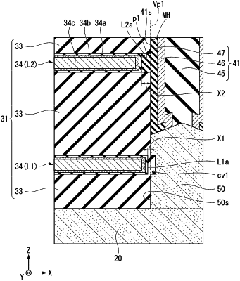
the first columnar body includes a semiconductor body and a charge accumulation film disposed between at least one of the plurality of conductive layers and the semiconductor body,
the plurality of conductive layers include a first conductive layer that surrounds an outer periphery of the first single-crystalline body and is closest to the substrate among the plurality of conductive layers surrounding the outer periphery of the first single-crystalline body, and a second conductive layer that surrounds an outer periphery of the first columnar body and is closest to the substrate among the plurality of conductive layers surrounding the outer periphery of the first columnar body,
an end of the first conductive layer is disposed outward of an outer side surface of the first single-crystalline body in a radial direction of the first columnar body with respect to the first columnar body,
an end of the second conductive layer is disposed outward of an outer side surface of the first columnar body in a radial direction of the first columnar body with respect to the first columnar body, and
the end of the second conductive layer is disposed outward of the end of the first conductive layer in a radial direction of the first columnar body with respect to the first columnar body;
a second columnar body extending in the first direction in the stacked body; and
a second single-crystalline body connected to an end of the second columnar body and disposed between the second columnar body and the substrate, wherein
the stacked body includes a cell array region and a stepped region,
the stepped region includes the plurality of first insulating layers and a plurality of second insulating layers alternately stacked therein,
the first columnar body is disposed in the cell array region,
the second columnar body is disposed in the stepped region, and
the plurality of second insulating layers include a third layer that surrounds the outer periphery of the second single-crystalline body and that is closest to the substrate among the plurality of second insulating layers, and a fourth layer that surrounds an outer periphery of the second columnar body and that is closest to the substrate among the plurality of second insulating layers,
an end of the fourth layer is disposed outward of an end of the third layer in a radial direction of the second columnar body with respect to the second columnar body.
|