| CPC H01L 23/49844 (2013.01) [H01L 23/49811 (2013.01); H01L 29/78 (2013.01)] | 20 Claims |
|
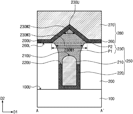
1. A method for forming a semiconductor device, the method comprising:
forming an interlayer insulating layer on a substrate;
forming a contact hole penetrating the interlayer insulating layer;
forming a lower pattern and a barrier pattern in the contact hole such that the barrier pattern is between the lower pattern and the interlayer insulating layer;
forming an upper insulating layer on the interlayer insulating layer such that the upper insulating layer covers topmost surfaces of the lower pattern and the barrier pattern;
forming a trench in the upper insulating layer such that the trench exposes the topmost surfaces of the lower pattern and the barrier pattern;
forming a recess region in the interlayer insulating layer by recessing the topmost surfaces of the lower pattern and the barrier pattern; and
forming an upper pattern filing the recess region,
wherein the upper pattern includes a protrusion protruding upwardly from a top surface of the interlayer insulating layer.
|