| CPC H01L 23/49838 (2013.01) [H01L 21/4857 (2013.01); H01L 23/49822 (2013.01); H01L 23/49816 (2013.01)] | 20 Claims |
|
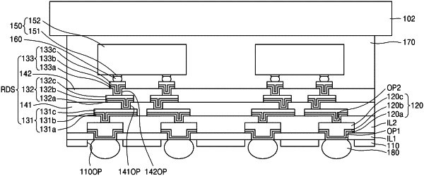
1. A method of manufacturing a semiconductor package, the method comprising:
forming a first insulating layer, the first insulating layer having a first opening;
forming a pad having an upper portion and a lower portion, the upper portion of the pad being located on the first insulating layer and the lower portion of the pad being located in the first opening;
forming a second insulating layer on the first insulating layer and the pad;
forming a redistribution structure on the second insulating layer;
attaching a semiconductor chip on the redistribution structure; and
forming a bump contacting a lower surface of the lower portion of the pad;
wherein the upper portion having a greater horizontal maximum length than the lower portion, and
wherein a lower surface of the first insulating layer and the lower surface of the lower portion of the pad are coplanar.
|