| CPC H01L 21/823481 (2013.01) [H01L 21/76224 (2013.01); H01L 21/823418 (2013.01); H01L 27/088 (2013.01); H01L 29/0847 (2013.01); H01L 21/823431 (2013.01); H01L 21/823456 (2013.01); H01L 21/823814 (2013.01); H01L 27/0886 (2013.01)] | 20 Claims |
|
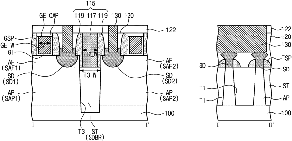
1. A semiconductor device comprising:
a device isolation layer provided on a substrate, the device isolation layer defining a first sub-active pattern and a second sub-active pattern, the first and second sub-active patterns extending in a first direction and spaced apart from each other in the first direction;
a first gate electrode and a second gate electrode crossing the first sub-active pattern and the second sub-active pattern, respectively; and
an isolation structure provided on the device isolation layer between the first and second sub-active patterns,
wherein the device isolation layer includes a diffusion break region disposed between the first and second sub-active patterns,
wherein the isolation structure covers a top surface of the diffusion break region,
wherein the isolation structure comprises:
an isolation pattern extending in a second direction crossing the first direction; and
isolation spacers provided on both sidewalls of the isolation pattern, respectively,
wherein the gate electrodes and the isolation pattern are formed of different materials from each other, and
wherein the isolation pattern has a first width that is the maximum width in the first direction, the diffusion break region has a second width that is the maximum width in the first direction, and the second width is greater than the first width.
|
|
7. A semiconductor device comprising:
a first fin-type active pattern formed on a substrate, the first fin-type active pattern extending in a first direction;
a second fin-type active pattern formed on the substrate, the second fin-type active pattern extending in the first direction;
the first and second fin-type active patterns spaced apart from each other in the first direction;
a device isolation layer disposed between the first and second fin-type active patterns, the device isolation layer being an insulator;
a first gate electrode and a second gate electrode crossing the respective first and second fin-type active patterns;
a first gate spacer disposed on one sidewall of the first gate electrode;
a second gate spacer disposed on the one sidewall of the second gate electrode; and
an isolation structure disposed on the device isolation layer between the first and second fin-type active patterns,
wherein the isolation structure comprises:
an isolation pattern extending in a second direction crossing the first direction; and
isolation spacers provided on both sidewalls of the isolation pattern, respectively,
wherein with respect to a vertical cross section taken along the first direction, the isolation pattern has a top surface at a location directly above a center of the device isolation layer at least as high as top surfaces of the first and second gate electrodes,
wherein the gate electrodes and the isolation pattern are formed of different materials from each other, and
wherein the isolation pattern has a first width that is the maximum width in the first direction, the diffusion break region has a second width that is the maximum width in the first direction, and the second width is greater than the first width.
|
|
13. A semiconductor device comprising:
a first fin-type active pattern formed on a substrate, the first fin-type active pattern extending in a first direction;
a second fin-type active pattern formed on the substrate, the second fin-type active pattern extending in the first direction;
the first and second fin-type active patterns spaced apart from each other in the first direction;
a device isolation layer disposed between the first and second fin-type active patterns, the device isolation layer being an insulator;
a first gate electrode and a second gate electrode crossing the respective first and second fin-type active patterns;
a first gate spacer disposed on one sidewall of the first gate electrode;
a second gate spacer disposed on the one sidewall of the second gate electrode; and
an isolation structure disposed on the device isolation layer between the first and second fin-type active patterns,
wherein the isolation structure comprises:
an isolation pattern extending in a second direction crossing the first direction; and
isolation spacers provided on both sidewalls of the isolation pattern, respectively,
wherein the gate electrodes and the isolation pattern are formed of different materials from each other, and
wherein the isolation pattern has a first width that is the maximum width in the first direction, the diffusion break region has a second width that is the maximum width in the first direction, and the second width is greater than the first width.
|