| CPC H01L 21/67727 (2013.01) [H01L 21/67736 (2013.01); H01L 21/68 (2013.01)] | 15 Claims |
|
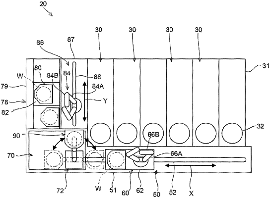
1. A substrate processing apparatus comprising:
at least one process chamber configured to be capable of processing a substrate;
one or more supports configured to be capable of supporting the substrate;
a transporter configured to be capable of transporting the one or more supports;
a transfer chamber configured to be capable of transferring the substrate;
a transport chamber that is adjacent to the transfer chamber and the at least one process chamber and is configured to be capable of moving the transporter; and
a delivery chamber configured to be capable of delivering the one or more supports,
wherein the delivery chamber includes at least two supporters, and
wherein the delivery chamber is configured such that a support of the one or more supports, which has been delivered from the transporter, is supported by one supporter of the at least two supporters, and a support of the one or more supports is supported by another supporter of the at least two supporters to allow the substrate to be transferred.
|