US 11,869,785 B2
Method of manufacturing semiconductor device and non-transitory computer-readable recording medium
Tomoyuki Miyada, Toyama (JP); Hajime Abiko, Toyama (JP); Junichi Kawasaki, Toyama (JP); and Tadashi Okazaki, Toyama (JP)
Assigned to Kokusai Electric Corporation, Tokyo (JP)
Filed by Kokusai Electric Corporation, Tokyo (JP)
Filed on Jan. 14, 2022, as Appl. No. 17/576,549.
Application 17/576,549 is a continuation of application No. 16/774,992, filed on Jan. 28, 2020, granted, now 11,257,699.
Application 16/774,992 is a continuation of application No. PCT/JP2017/027474, filed on Jul. 28, 2017.
Prior Publication US 2022/0139745 A1, May 5, 2022
Int. Cl. H01L 21/67 (2006.01); C23C 8/10 (2006.01); C23C 16/458 (2006.01); H01L 21/673 (2006.01); H01L 21/677 (2006.01); H01L 21/66 (2006.01)
CPC H01L 21/67288 (2013.01) [C23C 8/10 (2013.01); C23C 16/4587 (2013.01); H01L 21/67259 (2013.01); H01L 21/67303 (2013.01); H01L 21/67778 (2013.01); H01L 22/12 (2013.01)] 22 Claims
OG exemplary drawing
 
1. A method of manufacturing a semiconductor device, comprising:
(a) processing a substrate placed on a substrate retainer; and
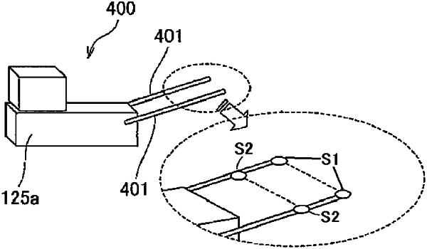
(b) detecting a state of abnormality of the substrate placed on the substrate retainer after the substrate retainer is rotated by a first angle with respect to a transferable position, wherein the substrate is transferable by a substrate transport device to/from the substrate retainer in the transferable position, wherein the state of abnormality comprises a state where the substrate jumps out from the substrate retainer toward the substrate transport device.