| CPC H01L 21/02568 (2013.01) [H01L 21/0242 (2013.01); H01L 21/02376 (2013.01); H01L 21/02417 (2013.01); H01L 21/02488 (2013.01); H01L 21/02631 (2013.01)] | 17 Claims |
|
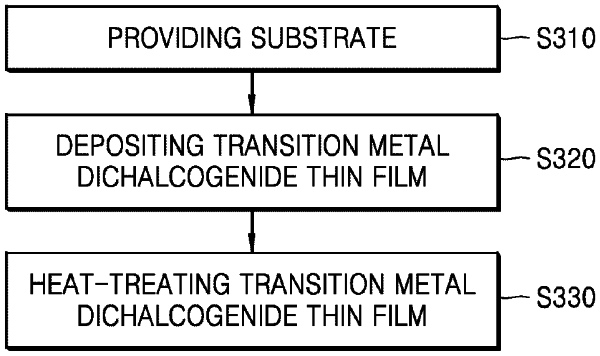
1. A method of forming a thin film of transition metal dichalcogenide, the method comprising:
providing a substrate in a reaction chamber;
depositing a transition metal dichalcogenide thin film on the substrate using a sputtering process that uses a transition metal precursor and a chalcogen precursor and is performed at a first temperature; and
injecting the chalcogen precursor in a gas state and heat-treating the transition metal dichalcogenide thin film at a second temperature that is higher than the first temperature,
wherein the first temperature is about 500° C. to about 800° C. and the second temperature is about 800° C. to about 1200° C., and
wherein a process pressure for the heat-treating the transition metal dichalcogenide thin film is about 1 torr to about 10 torr, and a deposition pressure for the depositing the transition metal dichalcogenide thin film on the substrate is about 0.1 mTorr to about 10 mTorr.
|