| CPC H01L 21/02293 (2013.01) [H01L 21/28518 (2013.01); H01L 21/76897 (2013.01); H01L 21/823431 (2013.01); H01L 21/823481 (2013.01); H01L 23/485 (2013.01); H01L 29/0673 (2013.01); H01L 29/0847 (2013.01); H01L 29/165 (2013.01); H01L 29/41766 (2013.01); H01L 29/41791 (2013.01); H01L 29/42392 (2013.01); H01L 29/6656 (2013.01); H01L 29/66439 (2013.01); H01L 29/66553 (2013.01); H01L 29/775 (2013.01); H01L 29/7848 (2013.01); H01L 29/78696 (2013.01)] | 20 Claims |
|
1. A semiconductor device, comprising:
a substrate;
an isolation layer on the substrate;
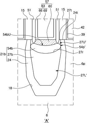
an active region penetrating through the isolation layer and extending in a first direction;
a source/drain on a first portion of the active region;
an interlayer insulating layer on the isolation layer and the source/drain;
a contact structure penetrating through the interlayer insulating layer and contacting the source/drain; and
an insulating spacer between the interlayer insulating layer and the contact structure,
wherein the source/drain includes:
a base epitaxial region on the first portion of the active region;
a first epitaxial region on the base epitaxial region and having a recessed surface; and
a second epitaxial region on the recessed surface of the first epitaxial region,
wherein the second epitaxial region vertically overlaps the insulating spacer and the contact structure,
wherein an upper end of the first epitaxial region is at a higher level than an upper end of the second epitaxial region,
wherein the insulating spacer contacts the first epitaxial region and the second epitaxial region, and
wherein the first direction is parallel to an upper surface of the substrate.
|