| CPC H01J 37/32651 (2013.01) [H01J 37/32568 (2013.01); H01J 37/32642 (2013.01); H01J 37/32935 (2013.01)] | 7 Claims |
|
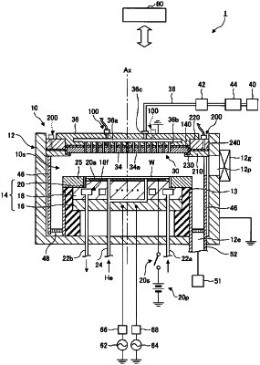
1. A plasma processing apparatus, comprising:
a processing chamber;
a placing table disposed in the processing chamber to place a substrate thereon;
an upper electrode facing the placing table;
a first member configured to adjust a temperature of the upper electrode;
a first sensor provided within the first member and configured to measure the temperature of the upper electrode; and
a first sheet member, disposed between the upper electrode and the first sensor, having a relative dielectric constant of 2.4 or higher at a frequency of 1 MHz, wherein a leading end of the first sensor is in contact with the first sheet member;
a ground electrode, disposed around the upper electrode, having a ground potential;
a second member configured to adjust a temperature of the ground electrode;
a second sensor provided within the second member and configured to measure the temperature of the ground electrode; and
a second sheet member, disposed between the ground electrode and the second sensor, having a relative dielectric constant of 2.4 or higher at a frequency of 1 MHz, wherein a leading end of the second sensor is in contact with the second sheet member.
|