| CPC H01J 37/32541 (2013.01) [H01J 37/32642 (2013.01); H01J 37/32715 (2013.01)] | 20 Claims |
|
1. A substrate processing method using a substrate processing apparatus, the substrate processing method comprising:
preparing a substrate;
forming a plasma; and
applying, by the substrate processing apparatus, a plasma-etching process to the substrate,
wherein the substrate processing apparatus includes an upper electrode, and the upper electrode includes:
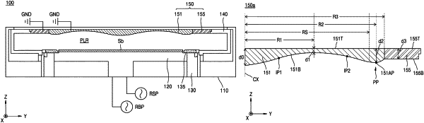
a bottom surface including a center region and an edge region, the edge region having a ring shape and surrounding the center region, and
a first protrusion portion protruding toward the plasma from the edge region and having the ring shape,
wherein the first protrusion portion includes a first apex corresponding to a local maximum thickness of the upper electrode in a vertical direction toward the plasma, the bottom surface configured to face the substrate with the plasma between, and
a first distance, which is a first radial-direction distance between the first apex and a center axis of the upper electrode, is greater than a radius of the substrate.
|