| CPC H01F 27/2804 (2013.01) [H01F 27/29 (2013.01); H01F 27/40 (2013.01); H01F 41/043 (2013.01); H01G 4/40 (2013.01); H01F 2027/2809 (2013.01)] | 19 Claims |
|
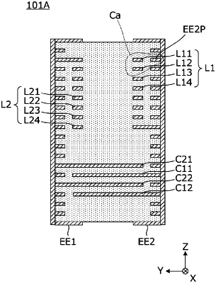
1. A circuit element comprising:
a multilayer body including insulating substrates;
a first coil conductor inside the multilayer body; and
a first outer electrode and a second outer electrode on an outer surface of the multilayer body; wherein
the first coil conductor includes a winding axis extending in a stacking direction of the insulating substrates;
the first coil conductor is connected to the first outer electrode or the second outer electrode;
the second outer electrode extends along a side surface of the multilayer body;
an additional capacitance is generated between the second outer electrode and the first coil conductor due to the second outer electrode and the first coil conductor being adjacent to or in a vicinity of each other;
the second outer electrode includes a first portion and a second portion having different widths from each other in a layer direction of the insulating substrates; and
the width of the second portion is larger than the width of the first portion.
|