| CPC G11C 16/26 (2013.01) [G06F 3/0604 (2013.01); G06F 3/0655 (2013.01); G06F 3/0679 (2013.01); G11C 16/0483 (2013.01); G11C 16/10 (2013.01); G11C 16/3459 (2013.01); H10B 69/00 (2023.02)] | 15 Claims |
|
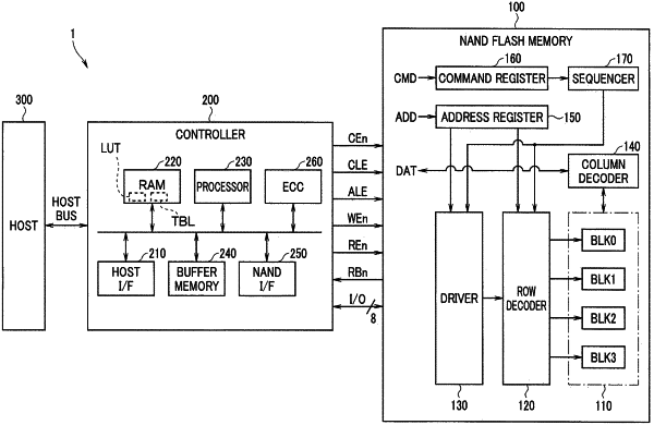
1. A method of controlling a memory device,
the memory device including:
a first memory including a storage area, the first memory being a nonvolatile memory;
a first data latch group used for input and output of data to and from the first memory; and
at least one second data latch group in which stored data is maintained when the data is read from the first memory, and
the method comprising:
storing management information in the at least one second data latch group when or before executing a read process for the data from the first memory, the management information being in a second memory and used for reading the data; and
executing the read process.
|