| CPC G11C 16/08 (2013.01) [G11C 16/26 (2013.01); H10B 41/41 (2023.02); H10B 43/40 (2023.02)] | 17 Claims |
|
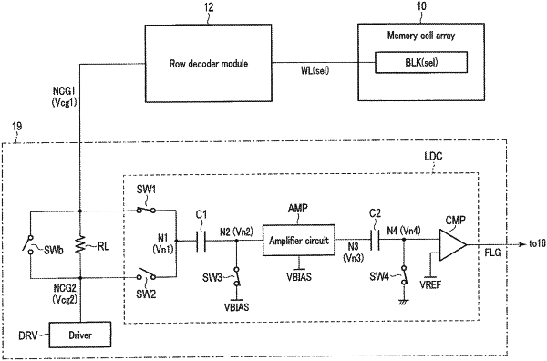
1. A semiconductor memory device, comprising:
a memory cell;
a first word line coupled between a control end of the memory cell and a first node;
a resistance element coupled between the first node and a second node;
a control circuit configured to output a voltage to the second node;
a first switch coupled between the first node and a third node;
a second switch coupled between the second node and the third node; and
a comparator including an input end that receives a signal corresponding to a voltage of the third node.
|