US 11,869,583 B2
Page write requirements for differing types of flash memory
Hari Kannan, Sunnyvale, CA (US); and Peter E. Kirkpatrick, Los Altos, CA (US)
Assigned to PURE STORAGE, INC., Santa Clara, CA (US)
Filed by Pure Storage, Inc., Mountain View, CA (US)
Filed on Mar. 25, 2022, as Appl. No. 17/704,747.
Application 17/704,747 is a continuation of application No. 17/085,362, filed on Oct. 30, 2020, granted, now 11,328,767.
Application 17/085,362 is a continuation of application No. 16/200,301, filed on Nov. 26, 2018, granted, now 10,832,767, issued on Nov. 10, 2020.
Application 16/200,301 is a continuation of application No. 15/498,979, filed on Apr. 27, 2017, granted, now 10,141,050, issued on Nov. 27, 2018.
Prior Publication US 2022/0215875 A1, Jul. 7, 2022
This patent is subject to a terminal disclaimer.
Int. Cl. G11C 11/34 (2006.01); G11C 11/56 (2006.01); G11C 16/10 (2006.01); G06F 3/06 (2006.01); G06F 12/02 (2006.01)
CPC G11C 11/5628 (2013.01) [G06F 3/061 (2013.01); G06F 3/0614 (2013.01); G06F 3/0656 (2013.01); G06F 3/0679 (2013.01); G06F 12/0246 (2013.01); G11C 16/10 (2013.01); G11C 16/102 (2013.01); G06F 2212/7203 (2013.01)] 18 Claims
OG exemplary drawing
 
1. A method, comprising:
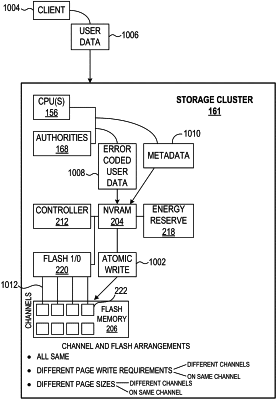
accumulating received data, in random-access memory (RAM) in a storage system to satisfy page write requirements for multi-level cell flash memory in the storage system; and
determining page write requirements for differing types of the multi-level cell flash memory within the storage system, the page write requirements providing an order for writing to pages of each of the differing types of the multi-level cell flash memory, wherein a source of the received data is external to the storage system and unaware of the page write requirements for the differing types of the multi-level cell flash memory.