| CPC G11C 11/4085 (2013.01) [G11C 5/06 (2013.01); G11C 11/4074 (2013.01); G11C 11/4087 (2013.01)] | 20 Claims |
|
1. An apparatus, comprising:
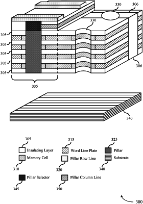
a first pillar extending through a stack of materials comprising a first word line plate comprising a first plurality of word lines and a second word line plate comprising a second plurality of word lines, wherein the first pillar is coupled with a first memory cell located between the first pillar and a first word line of the first plurality of word lines;
a second pillar extending though the stack of materials, wherein the second pillar is coupled with a second memory cell located between the second pillar and a second word line of the second plurality of word lines; and
an electrode coupled with the first word line plate and the second word line plate, the electrode operable to concurrently activate the first word line and the second word line to access the first memory cell and the second memory cell.
|