| CPC G11C 11/40615 (2013.01) [G11C 7/109 (2013.01); G11C 7/1063 (2013.01); G11C 11/4076 (2013.01); G11C 11/40622 (2013.01); G11C 16/3495 (2013.01); G06F 2212/1036 (2013.01)] | 20 Claims |
|
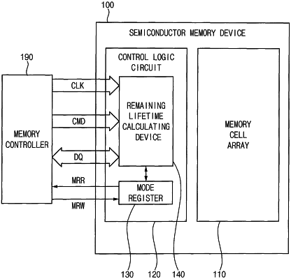
1. A semiconductor memory device comprising:
a memory cell array including a plurality of memory cells; and
a control logic circuit configured to receive a clock signal and a command from a memory controller, and to control the semiconductor memory device to transmit data stored in the memory cell array to the memory controller and/or to store the data received from the memory controller in the mentor cell array, the control logic circuit comprising:
a mode register; and
a remaining lifetime calculating device configured to count usage metrics based on one or more of the following:
a number of clock signals received from the memory controller,
an amount of data transmitted or received to or from the memory controller, and/or
a number of commands received from the memory controller,
wherein the control logic circuit generates a remaining lifetime code representing a remaining lifetime of the semiconductor memory device based on the usage metrics, and to store the remaining lifetime code in the mode register.
|