| CPC G09G 3/3266 (2013.01) [G09G 2300/0842 (2013.01); G09G 2310/0291 (2013.01)] | 20 Claims |
|
1. A display device comprising:
a display panel configured to display an image through sub pixels;
a scan driver embedded in the display panel and configured to supply a second scan signal to each of second gate lines connected to the sub pixels; and
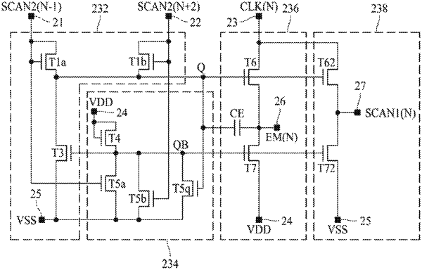
an emission control driver embedded in the display panel and configured to supply an emission control signal to each of third gate lines connected to the sub pixels, and supply a first scan signal to each of first gate lines connected to the sub pixels, the emission control driver comprising a plurality of emission control stages,
wherein each of the plurality of emission control stages includes:
an output buffer circuit configured to output the emission control signal to an output line and output the first scan signal to a scan output line by using a clock signal under control of a first control node, and configured to output a high potential power supply voltage to the output line and output a low potential power supply voltage to the scan output line under control of a second control node;
a charge/discharge circuit configured to charge the first control node by using the second scan signal supplied from the scan driver, and discharge the first control node by controlling the second control node; and
an inverter circuit configured to charge and discharge the second control node to be opposite to the first control node.
|