| CPC G09G 3/3233 (2013.01) [H10K 65/00 (2023.02); G06F 3/0412 (2013.01); G06F 3/0421 (2013.01); G06V 40/1318 (2022.01); G09G 2300/0426 (2013.01); G09G 2300/0852 (2013.01); G09G 2330/021 (2013.01); G09G 2354/00 (2013.01); G09G 2360/14 (2013.01)] | 14 Claims |
|
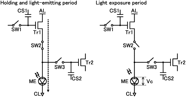
1. A display apparatus comprising:
first to third switches, a first transistor, a second transistor, and a light-emitting/receiving element,
wherein the first switch is electrically connected to a gate of the first transistor,
wherein the second switch is positioned between one of a source and a drain of the first transistor and one electrode of the light-emitting/receiving element,
wherein the third switch is positioned between the one electrode of the light-emitting/receiving element and a gate of the second transistor,
wherein the other of the source and the drain of the first transistor is supplied with a first potential,
wherein the other electrode of the light-emitting/receiving element is supplied with a second potential,
wherein the light-emitting/receiving element is configured to emit light of a first color and to receive light of a second color,
wherein in a period during which a potential is supplied to the gate of the first transistor, the first switch is on and the second switch is on or off,
wherein in a period during which the light-emitting/receiving element emits light, the second switch is on,
wherein in a period during which the light-emitting/receiving element receives light, the second switch is off and the third switch is off, and
wherein in a period during which electric charge is transferred from the light-emitting/receiving element to the gate of the second transistor, the second switch is off and the third switch is on.
|