| CPC G09G 3/32 (2013.01) [G09G 3/035 (2020.08); G09G 2300/0408 (2013.01); G09G 2300/0857 (2013.01); G09G 2310/0243 (2013.01); G09G 2310/08 (2013.01)] | 17 Claims |
|
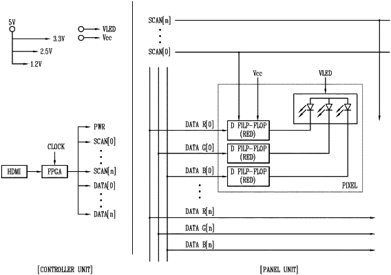
1. A display device comprising:
a plurality of semiconductor light-emitting elements disposed on a substrate;
flip-flops to apply an electric signal to the plurality of semiconductor light-emitting elements to allow the plurality of semiconductor light-emitting elements to maintain a light-emitting state for a predetermined time period;
scan electrodes and data electrodes electrically connected to each of the flip-flops, respectively; and
a driver that generates frame synchronization signals at a predetermined time interval of one frame and generates sub-field signals at a constant subfield time period obtained by dividing the predetermined time interval of one frame by a predetermined number, receives data packets corresponding to the one frame for a time corresponding to a multiple of the predetermined number of subfield time periods, and applies a voltage to a scan electrode and a data electrode from among the scan electrodes and the data electrodes based on the data packets.
wherein,
the sub-field signals generated during the predetermined time interval of one frame are generated so as not to be synchronized with the frame synchronization signals, and
when a frame synchronization signal from among the frame synchronization signals is generated during a time period from a time point at which a sub-field signal from among the sub-field signals is generated to a time point at which a next sub-field signal is generated, the driver prevents a voltage from being applied to the data electrodes by separately allocating extra bits for the time period from the time point at which the sub-field signal is generated to the time point at which the next sub-field signal is generated.
|