| CPC G09G 3/32 (2013.01) [G09G 2310/0256 (2013.01); G09G 2320/0257 (2013.01); G09G 2320/043 (2013.01)] | 11 Claims |
|
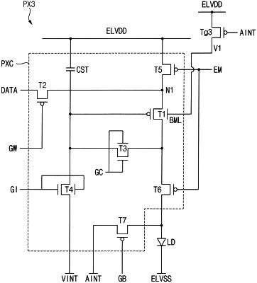
1. A pixel circuit comprising:
a first transistor including a first gate terminal, a first source terminal electrically connected to a first node, a first drain terminal electrically connected to a light emitting diode, and a back-gate terminal, wherein a first voltage which decreases over time is applied to the back-gate terminal;
a second transistor including a second gate terminal which receives a gate signal, a second source terminal which receives a data voltage, and a second drain terminal electrically connected to the first node; and
a global transistor including a global gate terminal which receives a second voltage that has a negative polarity, a global source terminal which receives a third voltage that has a positive polarity, and a global drain terminal electrically connected to the back-gate terminal,
wherein the global transistor is a single gate transistor.
|