| CPC G06F 7/502 (2013.01) [H03K 19/173 (2013.01); H03K 19/094 (2013.01)] | 9 Claims |
|
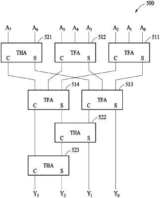
1. A circuit comprising:
a first full adder;
a second full adder;
a first half adder;
a third full adder configured to receive a sum output signal of the first full adder, a sum output signal of the second full adder, and a sum output signal of the first half adder;
a fourth full adder configured to receive a carry output signal of the first full adder, a carry output signal of the second full adder, and a carry output signal of the first half adder;
a second half adder configured to receive a carry output signal of the third full adder and a sum output signal of the fourth full adder; and
a third half adder configured to receive a carry output signal of the second half adder and a carry output signal of the fourth full adder,
wherein the third full adder, the second half adder, and the third half adder are configured to output voltage signals corresponding to a sum of logical values indicated by input signals applied to the first full adder, the second full adder, and the first half adder,
wherein the first full adder, the second full adder, the third full adder, and the fourth full adder are ternary full adders (TFAs), and
wherein the first half adder, the second half adder, and the third half adder are ternary half adders (THAs).
|