| CPC G06F 3/0655 (2013.01) [G06F 3/0604 (2013.01); G06F 3/0679 (2013.01); G06F 13/1668 (2013.01); G11C 7/1063 (2013.01); G11C 7/22 (2013.01)] | 9 Claims |
|
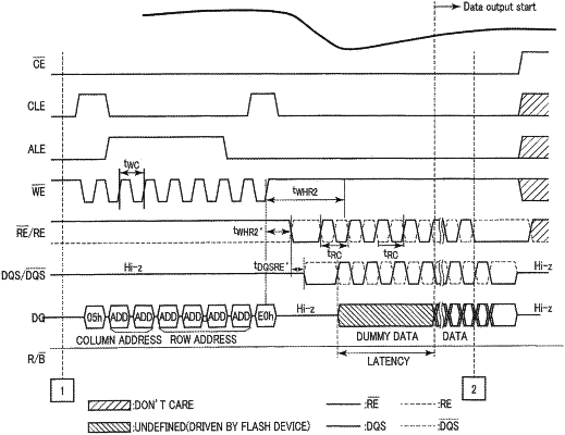
1. A memory system comprising:
a semiconductor memory; and
a controller configured to provide an instruction to read data from the semiconductor memory,
the semiconductor memory including,
a memory cell transistor configured to store data;
an output circuit configured to perform a process for data read from the memory cell transistor to be output to the controller; and
a data generator configured to generate first data,
wherein when the data is read,
the controller outputs a first signal to the semiconductor memory within a first period in which the output circuit is performing the process,
the semiconductor memory generates a second signal based on the first signal, and outputs the first data along with the second signal to the controller in the first period and a second period, and
after the second period has lapsed, the semiconductor memory outputs the data read from the memory cell transistor along with the second signal to the controller.
|