| CPC G02F 1/13312 (2021.01) [G02B 6/12009 (2013.01); G02B 6/29343 (2013.01); G02B 6/3546 (2013.01)] | 17 Claims |
|
1. A photodetection system comprising:
an optical scan device that includes:
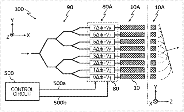
an optical waveguide array, including a plurality of optical waveguides and;
a phase shifter array including a plurality of phase shifters connected separately to each of the plurality of optical waveguides;
a control circuit that controls a phase shift amount of each of the plurality of phase shifters and/or inputting of light to each of the plurality of phase shifters and thereby controls a direction and shape of the light beam that is emitted from the optical scan device;
a photodetector that detects the light beam reflected by a physical object; and
a signal processing circuit that generates distance distribution data on the basis of output from the photodetector.
|