| CPC G01R 31/3274 (2013.01) [G01R 19/175 (2013.01)] | 25 Claims |
|
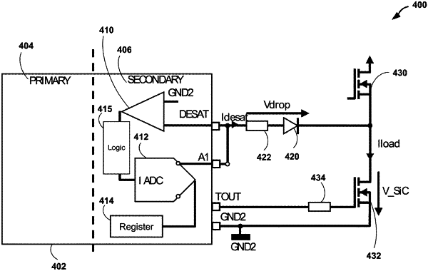
1. A driver circuit configured to control a power switch, the driver circuit comprising:
an output pin, wherein the driver circuit is configured to deliver drive signals from the output pin to the power switch to control ON/OFF switching of the power switch; and
a detection pin configured to receive a first signal associated with the power switch, wherein the first signal corresponds to a first point in time when current is not passing through the power switch and wherein the first signal indicates a first voltage drop over one or more other circuit elements,
wherein the detection pin is further configured to receive a second signal associated with the power switch, wherein the second signal corresponds to a second point in time when current is passing through the power switch and wherein the second signal indicates a voltage drop over the power switch in combination with a second voltage drop over one or more other circuit elements, and
wherein the driver circuit is configured to determine the voltage drop over the power switch based on a difference between the first signal and the second signal.
|