| CPC C30B 29/36 (2013.01) | 21 Claims |
|
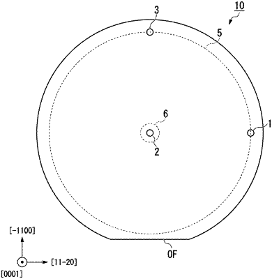
1. A SiC substrate,
wherein, in a case where a point 10 mm inside from an outer peripheral edge in a [11-20] direction from a center is defined as a first outer peripheral point and any point within a circle having a diameter of 10 mm from the center is defined as a first center point,
a tensile stress of the first outer peripheral point in a <1-100> direction, which is a circumferential direction of the first outer peripheral point, is larger than a tensile stress of the first center point in the <1-100> direction, which is the same direction as the circumferential direction of the first outer peripheral point,
the tensile stress of the first outer peripheral point in the circumferential direction of the first outer peripheral point is larger than the tensile stress of the first center point acting in the same direction as the circumferential direction of the first outer peripheral point by 10 MPa or more, and
the tensile stress is calculated as a product of a strain and a Young's modulus, the strain is obtained by (a0−a)/a0, a0 is a reference lattice constant, and a is a lattice constant obtained by an X-ray diffraction method.
|