| CPC B29C 64/268 (2017.08) [B33Y 30/00 (2014.12); B41J 2/0057 (2013.01); B41J 2/455 (2013.01); G02B 3/0087 (2013.01); G02B 3/06 (2013.01); G02B 19/0009 (2013.01); G02B 19/0047 (2013.01); H01S 5/02469 (2013.01); H01S 5/1833 (2013.01); H01S 5/18311 (2013.01); H01S 5/4018 (2013.01); H01S 5/426 (2013.01)] | 18 Claims |
|
1. A printing system comprising:
a writing module;
a member having an imaging surface configured to carry a layer of particles of a radiation modifiable material, the member and the writing module being movable relative to each other;
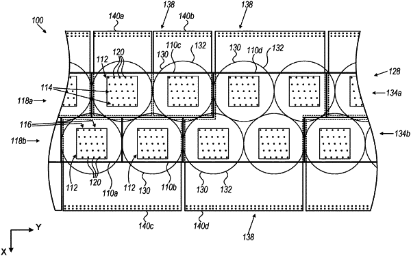
the writing module comprising a plurality of integrated electronic modules each having an array having a plurality of individually controllable light sources;
each controllable light source comprising a cascade of at least two Vertical-Cavity Surface-Emitting Laser (VCSEL) light-emitting semiconductor junctions connected in series with one another and disposed to emit light along a common axis so as to direct a single beam onto a single spot on the imaging surface;
the plurality of spots from the respective plurality of light sources being spaced from one another in a direction transverse to the direction of movement between the writing module and the imaging surface.
|