| CPC A61B 8/4494 (2013.01) [A61B 5/6848 (2013.01); A61B 8/0841 (2013.01); A61B 17/3417 (2013.01); A61B 90/39 (2016.02); B06B 1/0688 (2013.01); A61B 8/4444 (2013.01); A61B 17/3403 (2013.01); A61B 2017/00526 (2013.01); A61B 2017/3413 (2013.01); A61B 2090/3925 (2016.02); A61B 2090/3929 (2016.02); A61B 2562/164 (2013.01)] | 20 Claims |
|
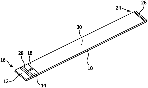
1. A sensor device for applying a sensor to a medical device, the sensor device comprising:
a flexible planar strip configured to at least partially encapsulate the medical device, the flexible planar strip comprising:
a first dielectric layer;
a second dielectric layer;
a patterned conductive layer disposed on the second dielectric layer, the patterned conductive layer including a sensor electrode disposed at a distal end portion of the patterned conductive layer, a hub electrode disposed at the proximal end of the patterned conductive layer, and a trace connecting the sensor electrode and the hub electrode;
an ultrasound sensor disposed on the sensor electrode, a first surface of the ultrasound sensor configured to make electrical contact with the sensor electrode and a second surface of the ultrasound sensor exposed for making electrical contact with the medical device; and
a third dielectric layer formed on the patterned conductive layer, wherein a distal end portion of the third dielectric layer is recessed to expose the sensor electrode and a proximal and portion of the third dielectric layer is recessed to expose the hub electrode.
|