| CPC H10K 59/122 (2023.02) [H10K 50/844 (2023.02); H10K 59/12 (2023.02); H10K 59/124 (2023.02); H10K 59/88 (2023.02)] | 27 Claims |

|
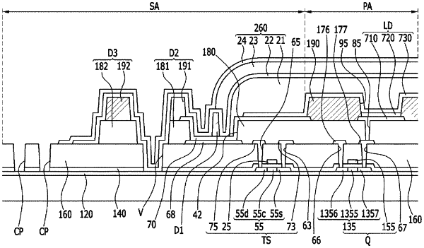
[ 7. An OLED display, comprising:
a flexible substrate having a pixel area;
a semiconductor layer formed in the pixel area and disposed on the flexible substrate;
a gate insulating layer disposed on the semiconductor and the flexible substrate;
a gate electrode disposed on the gate insulating layer;
a first interlayer insulating layer disposed on the gate electrode and the gate insulating layer;
a first electrode and a second electrode disposed on the first interlayer insulating layer;
a second interlayer insulating layer disposed on the first electrode and the second electrode;
a first emission electrode electrically connected to the second electrode on the second interlayer insulating layer;
a pixel defined layer having an opening and disposed on the second interlayer insulating layer exposing the first electrode;
an organic emission layer disposed on the first emission electrode;
a second emission electrode disposed on the organic emission layer;
a first inorganic insulating layer disposed over the second emission electrode;
an organic insulating layer disposed over the first inorganic insulating layer;
a first dam comprised of a pattern of the pixel defined layer disposed along an edge of the flexible substrate; and
a first groove disposed through the first interlayer insulating layer between the first dam and the edge of the flexible substrate; wherein the first inorganic insulating layer does not cover over the first groove,
wherein the organic insulating layer does not cover over the first dam.]
|