| CPC H10N 70/8265 (2023.02) [H10B 63/845 (2023.02); H10N 70/841 (2023.02); H10N 70/8836 (2023.02); H10N 70/884 (2023.02); H01L 29/4234 (2013.01)] | 16 Claims |

|
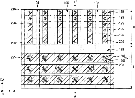
1. A vertical variable resistance memory device, comprising:
gate electrodes spaced apart from each other in a first direction on a substrate to form a plurality of gate electrode structures, each of the gate electrodes including graphene and extending in a second direction, the first direction being substantially perpendicular to an upper surface of the substrate and the second direction being substantially parallel to the upper surface of the substrate;
first insulation patterns between the gate electrodes, each of the first insulation patterns including boron nitride (BN);
second insulation patterns between the gate electrodes and extending along the first direction into the substrate, and each of the second insulation patterns including amorphous boron nitride and being in direct contact with the substrate; and
pillar structures extending in the first direction through the gate electrodes and the first insulation patterns on the substrate, each of the pillar structures includes a vertical gate electrode extending in the first direction and a variable resistance pattern on a sidewall of the vertical gate electrode;
first wirings electrically connected to the plurality of gate electrode structures, each of the first wirings extending in the second direction on the plurality of gate electrode structures; and
second wirings electrically connected to the vertical gate electrodes of the pillar structures, each of the second wirings extending in a third direction on the pillar structures to overlap the second insulation patterns, the third direction being substantially parallel to the upper surface of the substrate and crossing the second direction,
wherein the first insulation patterns include amorphous boron nitride (a-BN); and
wherein each of the second insulation patterns has an extension extending continuously in the second direction between the pillar structures that are spaced apart from each other along a third direction crossing to the second direction.
|