| CPC H10K 59/88 (2023.02) [H10K 59/1213 (2023.02); H10K 59/1216 (2023.02); H10K 59/122 (2023.02); H10K 59/131 (2023.02)] | 20 Claims |

|
1. A display panel comprising:
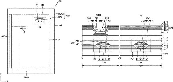
a substrate including a first region, a second region, a non-display area that surrounds the first region and the second region, and a display area that surrounds the non-display area;
a plurality of display elements on the display area;
a plurality of pixel circuits connected to the each of the plurality of display elements on the display area;
a plurality of dummy pixel circuits disposed on the non-display area;
a pixel defining layer disposed over the plurality of pixel circuits and the plurality of dummy pixel circuits,
wherein the pixel defining layer comprises a plurality of openings corresponding to each of the plurality of display elements, and
wherein the pixel defining layer entirely covers the non-display area and has a flat upper surface on an area corresponding to the plurality of dummy pixel circuits.
|