| CPC H10K 59/131 (2023.02) [H10K 59/18 (2023.02); G02F 1/13336 (2013.01); G06F 3/1446 (2013.01); G09F 9/3026 (2013.01); G09G 2300/026 (2013.01); G09G 2300/0408 (2013.01); G09G 2300/0804 (2013.01); H10K 50/15 (2023.02); H10K 50/16 (2023.02); H10K 50/17 (2023.02); H10K 50/171 (2023.02); H10K 50/818 (2023.02); H10K 50/828 (2023.02); H10K 50/8426 (2023.02); H10K 50/844 (2023.02); H10K 59/121 (2023.02); H10K 59/1216 (2023.02); H10K 59/127 (2023.02); H10K 59/1275 (2023.02); H10K 59/128 (2023.02); H10K 59/176 (2023.02); H10K 59/35 (2023.02); H10K 77/111 (2023.02); H10K 2102/00 (2023.02); H10K 2102/311 (2023.02)] | 22 Claims |
|
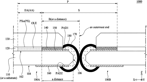
1. A display device, comprising:
a substrate including an active area,
a plurality of pixels in the active area, each of the pixels of the plurality being spaced a selected distance apart from an adjacent pixel of the plurality; and
a gate driving circuit disposed between the plurality of pixels in the active area,
wherein each of the plurality of pixels include an emission area including an organic light emitting layer, and
wherein a distance between a side surface of the substrate and the emission area of an outermost pixel among the plurality of pixels is either equal to or smaller than half of the selected distance between the adjacent pixels.
|