| CPC H10K 59/131 (2023.02) [H10K 59/1216 (2023.02)] | 19 Claims |

|
1. A display substrate, comprising:
a base substrate, comprising:
a first opening region comprising a first opening and a first opening peripheral region surrounding the first opening;
a second opening region which is adjacent to the first opening region in a first direction and comprises a second opening and a second opening peripheral region surrounding the second opening;
an inter-opening region between the first opening region and the second opening region, wherein at least one selected from a group consisting of the inter-opening region, the first opening peripheral region, and the second opening peripheral region comprises a first dummy sub-pixel;
a display region which at least partially surrounds the first opening region, the second opening region, and the inter-opening region, and comprises a plurality of pixels, wherein each of the plurality of pixels comprises a plurality of sub-pixels, each of the plurality of sub-pixels comprises a pixel circuit, and the pixel circuit comprises:
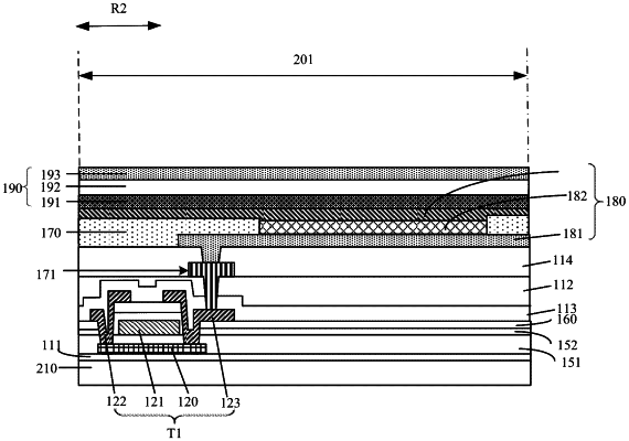
a transistor comprising an active layer, a gate electrode, and a source electrode and a drain electrode;
a light-emitting element connected with one of the source electrode and the drain electrode of the transistor; and
a storage capacitor comprising a first electrode plate and a second electrode plate, wherein the gate electrode and the first electrode plate of the storage capacitor are in a same layer; and
a first signal line which extends in the first direction, comprises a first portion passing through the first opening peripheral region, the inter-opening region, and the second opening peripheral region, and is configured to provide a first display signal to the pixel circuit, wherein the first portion of the first signal line passes through the first dummy sub-pixel, the first dummy sub-pixel comprises a virtual pixel circuit, the virtual pixel circuit comprises a first compensation capacitor, and the first compensation capacitor comprises:
a first electrode plate which is in a same layer as the first portion of the first signal line and electrically connected with the first signal line, and is in a same layer as the second electrode plate of the storage capacitor; and
a second electrode plate which is in a different layer and insulated from the first electrode plate of the first compensation capacitor, wherein an orthographic projection of the second electrode plate of the first compensation capacitor on the base substrate at least partially overlaps with an orthographic projection of the first electrode plate of the first compensation capacitor on the base substrate, wherein
the first electrode plate of the first compensation capacitor comprises:
a first extension portion which is connected with the first portion of the first signal line, extends from the first portion of the first signal line and is at a first side of the first portion of the first signal line in a second direction intersecting with the first direction; and
a second extension portion which is connected with the first portion of the first signal line, extends from the first portion of the first signal line and is at a second side of the first portion of the first signal line opposite to the first side in the second direction.
|