| CPC H10K 59/122 (2023.02) [H10K 50/824 (2023.02); H10K 59/1213 (2023.02); H10K 59/124 (2023.02); H10K 59/38 (2023.02); H10K 71/00 (2023.02); H01L 27/1214 (2013.01); H10K 59/1201 (2023.02)] | 19 Claims |

|
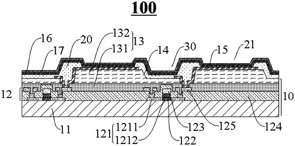
1. A display substrate comprising:
a first substrate;
a pixel defining layer on the first substrate and comprising a plurality of sub-pixel openings;
an insulating layer between the first substrate and the pixel defining layer and comprising a groove;
a circuit structure layer between the first substrate and the insulating layer; and
at least one recess on a side of the display substrate away from the first substrate,
wherein an orthographic projection of the at least one recess on the first substrate and orthographic projections of the plurality of sub-pixel openings on the first substrate do not overlap,
wherein the insulating layer comprises a passivation layer and a first flat layer that are stacked, the passivation layer is between the circuit structure layer and the first flat layer, and
wherein a bottom of the groove is in the first flat layer, or the bottom of the groove is at an interface between the first flat layer and the passivation layer, or the bottom of the groove is in the passivation layer and does not penetrate the passivation layer.
|