US 12,193,272 B2
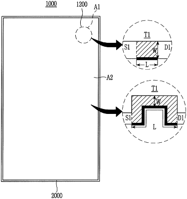
Display device having transistors with bent regions and other transistors without bent regions
Jin Woo Park, Yongin-si (KR); Won Kyu Kwak, Yongin-si (KR); Dong Wook Kim, Yongin-si (KR); and Hyun-Chol Bang, Yongin-si (KR)
Assigned to SAMSUNG DISPLAY CO., LTD., Yongin-si (KR)
Filed by Samsung Display Co., Ltd., Yongin-si (KR)
Filed on Aug. 21, 2023, as Appl. No. 18/453,037.
Application 18/453,037 is a continuation of application No. 16/684,944, filed on Nov. 15, 2019, granted, now 11,818,917.
Claims priority of application No. 10-2018-0140835 (KR), filed on Nov. 15, 2018.
Prior Publication US 2023/0397456 A1, Dec. 7, 2023
This patent is subject to a terminal disclaimer.
Int. Cl. G09G 3/32 (2016.01); G09G 3/20 (2006.01); G09G 3/3225 (2016.01); H10K 59/121 (2023.01); H10K 59/126 (2023.01); H10K 59/38 (2023.01); H10K 59/131 (2023.01)
CPC H10K 59/1213 (2023.02) [G09G 3/2003 (2013.01); G09G 3/3225 (2013.01); H10K 59/126 (2023.02); H10K 59/38 (2023.02); G09G 2360/145 (2013.01); H10K 59/131 (2023.02)] 14 Claims
OG exemplary drawing
 
1. A display device, comprising:
a display panel including a plurality of transistors and displaying an image on a front surface thereof; and
a sensing module on a rear surface of the display panel,
wherein:
the display panel includes a first region that overlaps the sensing module and a second region that does not overlap the sensing module,
the transistors in the second region each include a bent region between a source and a drain, and the transistors in the first region do not include a bent region, and
the number of transistors with bent regions is greater than the number of transistors with non-bent regions.