| CPC H10K 59/1213 (2023.02) [H01L 27/1262 (2013.01); H10K 50/844 (2023.02); H10K 59/1201 (2023.02)] | 28 Claims |

|
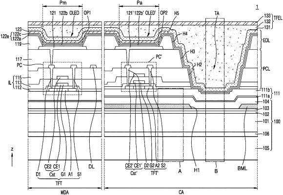
1. A display apparatus comprising:
a main display area; and
a component area comprising pixel groups spaced apart from each other and a transmission area between the pixel groups,
the display apparatus further comprising:
a substrate comprising a first base layer, a compensation layer, a first barrier layer, and a second barrier layer sequentially stacked on one another;
a bottom metal layer between the first barrier layer and the second barrier layer;
a buffer layer above the second barrier layer;
main display elements on the substrate of the main display area;
auxiliary display elements on the substrate of the component area; and
a thin film transistor comprising a semiconductor layer above the buffer layer,
wherein the buffer layer comprises:
a first buffer layer having a thickness of 80 Å to 250 Å; and
a second buffer layer on the first buffer layer and having a thickness of 1,000 Å to 4,000 Å,
wherein the second barrier layer comprises a first layer and a second layer on the first layer, and
wherein the second layer is greater in amount of chlorine than the first layer.
|