| CPC H10K 50/865 (2023.02) [G02F 1/133331 (2021.01); G02F 1/133512 (2013.01); G02F 1/136209 (2013.01); G02F 2201/121 (2013.01); G02F 2201/123 (2013.01); G02F 2201/501 (2013.01); G02F 2202/28 (2013.01)] | 27 Claims |

|
1. A display device comprising:
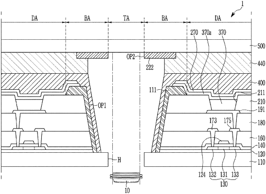
a substrate that overlaps a light transmission area, a display area that surrounds the light transmission area, and a boundary area that is disposed between the light transmission area and the display area;
an insulation layer overlapping the boundary area and the display area and defining a hole overlapping the light transmission area;
a pixel electrode disposed on the insulation layer,
an emission layer disposed on the pixel electrode,
a common electrode disposed on the emission layer,
an encapsulation layer disposed on the common electrode, and
a first light blocking layer disposed on an inner surface of the hole,
wherein the first light blocking layer contacts an upper surface of the substrate and the encapsulation layer.
|