| CPC H10K 50/844 (2023.02) [H10K 59/131 (2023.02); G02F 1/133305 (2013.01); G02F 1/133331 (2021.01); G02F 1/133512 (2013.01); G02F 1/133514 (2013.01); G02F 1/133528 (2013.01); G02F 1/136209 (2013.01); G06F 1/1652 (2013.01); G09F 9/301 (2013.01); G09G 2330/02 (2013.01); G09G 2380/02 (2013.01); H01L 27/14678 (2013.01); H10K 50/8426 (2023.02); H10K 50/865 (2023.02); H10K 50/868 (2023.02); H10K 59/12 (2023.02); H10K 59/1213 (2023.02); H10K 59/1216 (2023.02); H10K 59/123 (2023.02); H10K 59/126 (2023.02); H10K 59/35 (2023.02); H10K 59/352 (2023.02); H10K 59/38 (2023.02); H10K 59/40 (2023.02); H10K 59/8792 (2023.02); H10K 77/111 (2023.02); H10K 2102/311 (2023.02)] | 14 Claims |

|
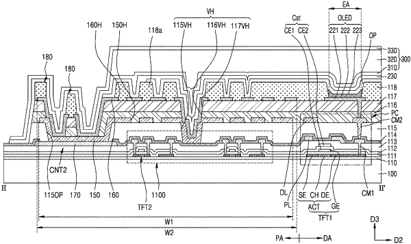
1. A display apparatus comprising a display area and a peripheral area outside the display area, the display apparatus comprising:
a first conductive layer on a substrate in the peripheral area and comprising a first hole;
a second conductive layer on the first conductive layer in the peripheral area;
a first insulating layer on the second conductive layer in the peripheral area;
a display element in the display area and comprising a first electrode, a second electrode facing the first electrode, and an emission layer between the first electrode and the second electrode,
wherein the second electrode comprises a portion in the peripheral area, and
wherein a first contact area of a plurality of contact areas at which the portion of the second electrode contacts the second conductive layer overlaps the first hole of the first conductive layer, and a second contact area of the plurality of contact areas contacts the first conductive layer;
a second insulating layer between the first conductive layer and the second conductive layer; and
a third insulating layer between the second insulating layer and the first electrode in the display area.
|