| CPC H10K 39/32 (2023.02) [H10K 30/30 (2023.02)] | 20 Claims |

|
1. An imaging device comprising:
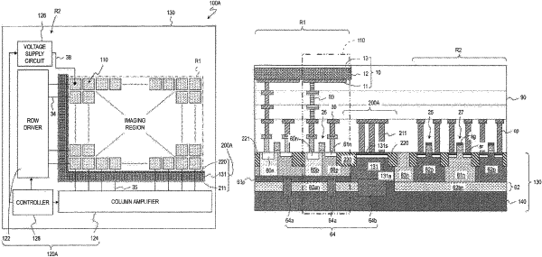
an imaging region including a plurality of pixels, each pixel including a photoelectric converter to generate a charge;
a first doped region electrically connected to the photoelectric converter;
a peripheral region located outside of the imaging region, with a circuit to drive the plurality of pixels being provided in the peripheral region;
a second doped region of a first conductivity type located between the imaging region and the peripheral region; and a plurality of first contact plugs connected to the second doped region;
a third doped region of a second conductivity type located between the peripheral region and the second doped region; and a plurality of second contact plugs provided in the third doped region, and
a semiconductor substrate having the first doped regions, the second doped region, and the third doped region, wherein
the semiconductor substrate further includes, inside the semiconductor substrate, an impurity layer of the second conductivity type that is located in a position deeper than the first doped regions; and
the third doped region includes two portions each extending, in a cross section perpendicular to a surface of the semiconductor substrate, from the surface and reaching the impurity layer.
|
|
17. An imaging device having a plurality of pixels, the imaging device comprising:
a semiconductor substrate in which a plurality of doped regions are provided; and
a photoelectric converter to generate a charge, wherein,
each pixel includes:
a portion of the photoelectric converter;
one of the plurality of doped regions; and
a contact plug electrically connected to the one of the plurality of doped regions; and
the semiconductor substrate includes a carbon-containing layer that contains carbon, the carbon-containing layer being located between the doped regions and the contact plugs.
|
|
19. An imaging device comprising:
an imaging region including a plurality of pixels, each pixel including a photoelectric converter to generate a charge, and a first doped region electrically connected to the photoelectric converter;
a peripheral region located outside of the imaging region, with a circuit to drive the plurality of pixels being provided in the peripheral region;
a second doped region of a first conductivity type located between the imaging region and the peripheral region;
a plurality of first contact plugs connected to the second doped region, and
a carbon-containing layer that contains carbon, the carbon-containing layer being located below the plurality of first contact plugs.
|